Microfluidic chips integrate sample preparation, biochemical reactions and result detection steps into a very small plastic-based chip, so that the amount of reagents used for detection can be microliters or even nanoliters or picoliters. In addition to using a small amount of reagents, microfluidic chips also have the advantages of fast reaction speed and disposable.
Microfluidic chips are a project that has been vigorously developed in China in recent years. Microfluidic chips are actually a miniature diagnostic platform that can quickly diagnose diseases and save a lot of manpower and material resources. At the same time, the microfluidic chip diagnostic platform is easy to carry and is suitable for rapid diagnosis of diseases in underdeveloped or remote areas. Microfluidic chips are very easy to use, but producing them is not an easy task.
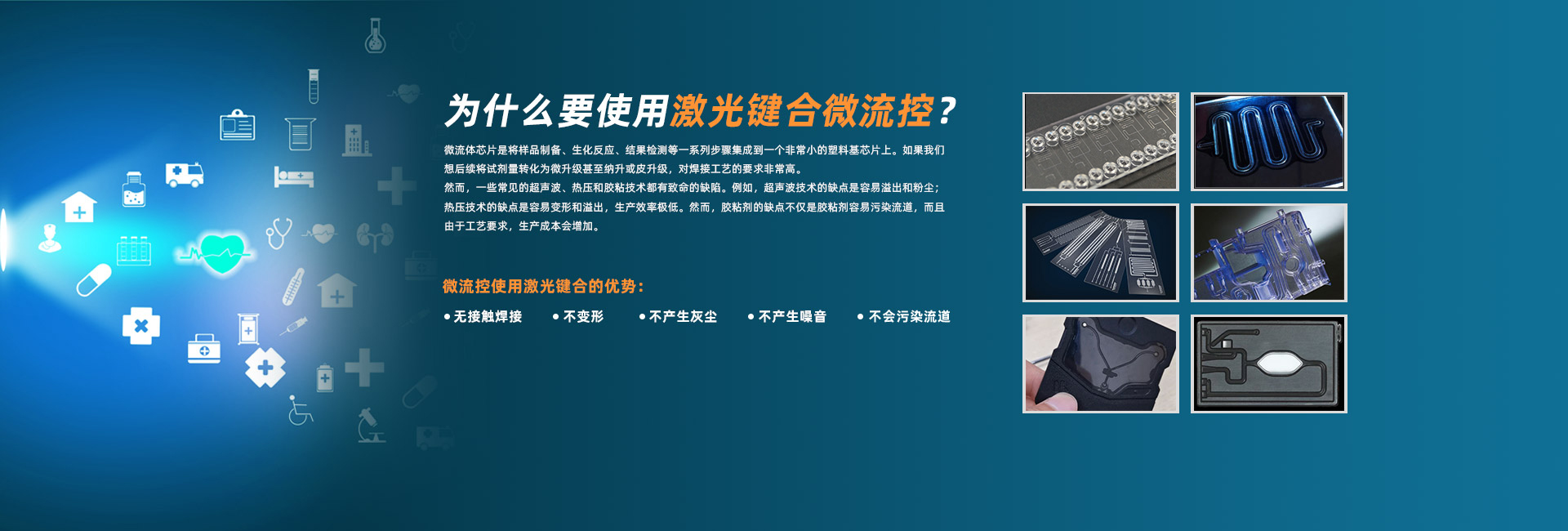
Microfluidic chips are composed of a cover sheet and a glass slide. The cover sheet is a plastic film or a plastic sheet with a thickness of several millimeters; many complex precision flow channels are formed on the glass slide through engraving or injection molding, and the width of the flow channels is generally about 100 microns to 1 millimeter. To seal these precision flow channels, the common processes mainly include ultrasonic, hot pressing and glue bonding processes, and these processes all have fatal defects. The ultrasonic process will produce large overflow and dust, destroying and polluting the flow channel; the heat-affected zone of the hot pressing process is too large, which is easy to deform and overflow, destroying the flow channel structure, and the production efficiency of the hot pressing process is very low; glue bonding will cause glue to enter the flow channel and pollute the flow channel. At the same time, production requires additional dispensing and glue curing processes, which increases costs. To solve the above problems, the most reliable process is plastic laser welding. The laser welding process used for microfluidic chips is mainly the mask welding process of Laiser Laser.
The mask welding process uses a linear laser beam and a mask to partially shield the flow channel. The laser beam scans the chip and the parts that need to be welded are welded, while the flow channel will not be affected by the mask blocking the laser. The welding accuracy of mask welding (from the edge of the weld line to the flow channel) can reach about 0.1mm, which can meet the requirements of most microfluidic chips used in clinical practice.


![Plastic laser welding machine_Laser die cutting machine_Automatic laser engraving [Laiser Laser]](https://www.lasertic.com/uploads/3/images/sousuo1.png)
